
The "photonic VRAM issue" is real, quantified, and structural — but silicon photonics does not resolve it in one move. It resolves it across three staged horizons, and only the first is deployable today. This is a verified investigation: every figure below traces to a peer-reviewed or primary source, and the four most attractive vendor claims we found were adversarially refuted and excluded from the recommendations.
The clean way to see it: photonics first fixes the interconnect (energy-per-bit and reach), which indirectly buys back VRAM capacity by freeing die-edge real estate. Only later does it fix memory placement through optical disaggregation and pooling — the actual "photonic VRAM" payoff. Photonic memory itself (optical RAM, in-memory compute) remains a research bet.
Bottom line. Deploy co-packaged / optical I/O for the scale-up/scale-out fabric now (it also frees beachfront for more local HBM); move to optically pooled HBM next, accepting a ~200 ns access tax for capacity elasticity; treat photonic in-memory compute as a hedge, not a plan. Standardize on UCIe-optical + CXL semantics to avoid lock-in.
1. The Problem, Quantified
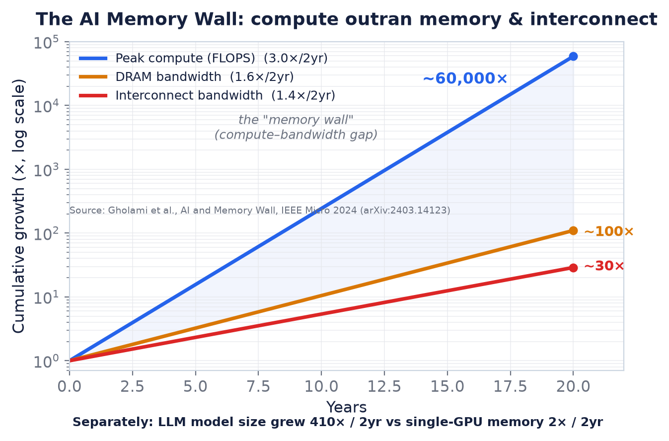
The bottleneck is a memory-and-interconnect wall, not a compute wall. Over roughly 20 years (Gholami et al., AI and Memory Wall, IEEE Micro 2024), the scaling rates diverged sharply.
| Axis | Growth / 2 yr | 20-yr total | Verdict |
|---|---|---|---|
| Peak server compute (FLOPS) | 3.0× | ~60,000× | runs ahead |
| DRAM bandwidth | 1.6× | ~100× | falls behind |
| Interconnect bandwidth | 1.4× | ~30× | falls furthest |
Compute outran memory bandwidth by ~600× and interconnect by ~2,000×. Layered on top: LLM model size grew 410× / 2 yr while single-GPU memory grew only 2× / 2 yr. That gap forces models to be split across many accelerators — converting a capacity problem into an interconnect problem, which is exactly where photonics has leverage. (Caveat carried from verification: the 410× figure reflects flagship/MoE models and overstates dense-model growth — but the gap is the point.)
2. Why HBM + Electrical SerDes Can't Close It Alone
Two physical ceilings, both about the die edge — the perimeter engineers call the "beachfront":
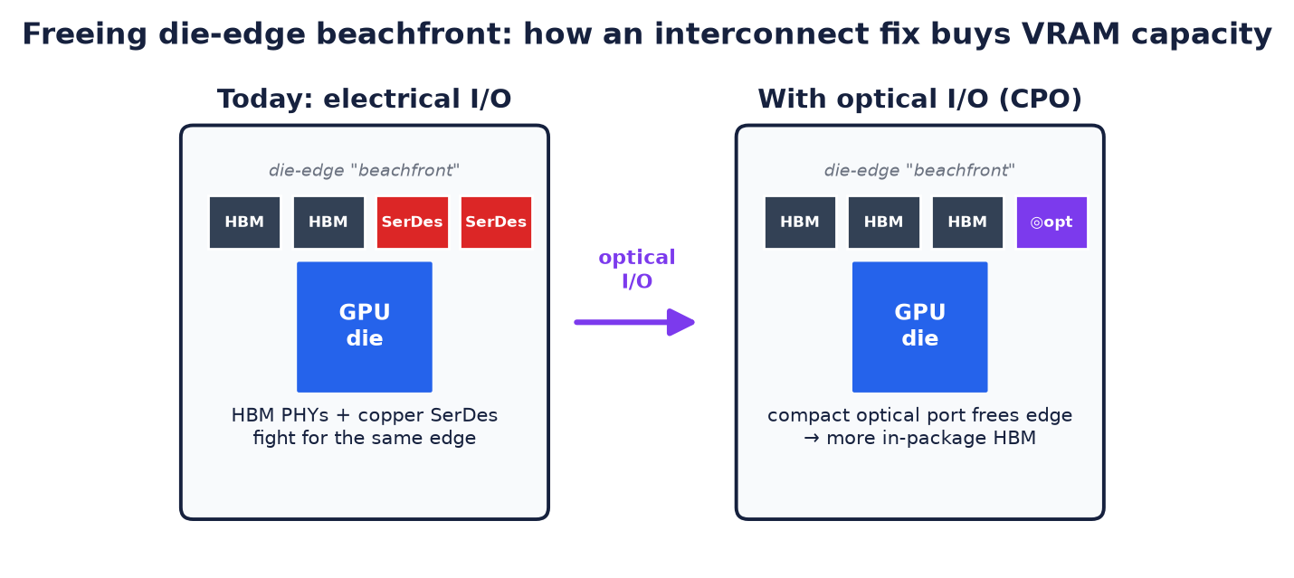
- Compute scales with die area; I/O scales with die perimeter. HBM PHYs and electrical SerDes compete for the same finite shoreline — you can't add memory stacks and more copper I/O indefinitely.
- Electrical SerDes hit an energy-per-bit and reach wall (multi-pJ/bit, ~tens of cm). Push bandwidth up and power density and signal integrity collapse. This is why in-rack copper is topping out.
The consequence: HBM3E→HBM4 keeps stacking, but the ratio of memory to compute is welded into the package, and the interconnect that would let you pool memory across packages is electrically capped. The verified industry mechanism — making the optical connection directly into the XPU "frees up highly valuable die-edge beachfront, which can be repurposed to significantly increase the amount of HBM within the XPU package" — is how an interconnect technology buys capacity.
3. The Photonic Toolbox — What Each Approach Actually Does
| Approach | What it does | Fixes | Maturity |
|---|---|---|---|
| Ayar Labs TeraPHY (UCIe optical chiplet) | Replaces edge SerDes with DWDM optical I/O; up to 8 Tbps, 16-λ SuperNova laser, ~5 pJ/bit; first UCIe optical chiplet → multi-vendor, protocol-agnostic | Link energy + reach; frees beachfront | Product / near-term |
| Celestial AI Photonic Fabric (acq. Marvell, Dec 2025) | Optical chip-to-chip and chip-to-memory; 16 Tbps/chiplet; Gen1 module ~2.07 TB pooled, 7.2 Tbps, ~200 ns | Disaggregation / HBM pooling | Design-in / medium-term |
| Lightmatter Passage | 3D photonic interposer + CPO, high-density DWDM | Package bandwidth density | Emerging |
| Nvidia / TSMC CPO roadmap | Co-packaged optics for scale-up/scale-out switching | Fabric power + radix | 2026-era |
| Optical CXL / memory pooling | Rack-scale memory pools over CXL semantics | Capacity elasticity | Emerging |
| Photonic in-memory compute (pSRAM) | Compute in the optical domain, ~2.5 TOPS/W | Memory–compute round trips | Research |
4. Quantitative Feasibility (the Calculation)
4.1 Energy per bit — the decisive metric
Electrical SerDes sit at multiple pJ/bit. Peer-reviewed optical link electronics are in the sub-pJ/bit regime: a 3D-integrated microresonator link achieves ~120 fJ/bit total (50 fJ/bit TX at 1 V swing + 70 fJ/bit RX; Nature Photonics 2025), and DWDM thermal-tuning drops to ~313–334 fJ/bit (IEEE CICC 2024).
4.2 Bandwidth density — where electrical can't follow
Shoreline density reaches ~2.02 Tbps/mm (16.384 Tbps out an 8.10 mm edge; CICC 2024) and area density 5.3 Tb/s/mm² (3D transceiver; Nature Photonics 2025) — both beyond practical electrical limits.
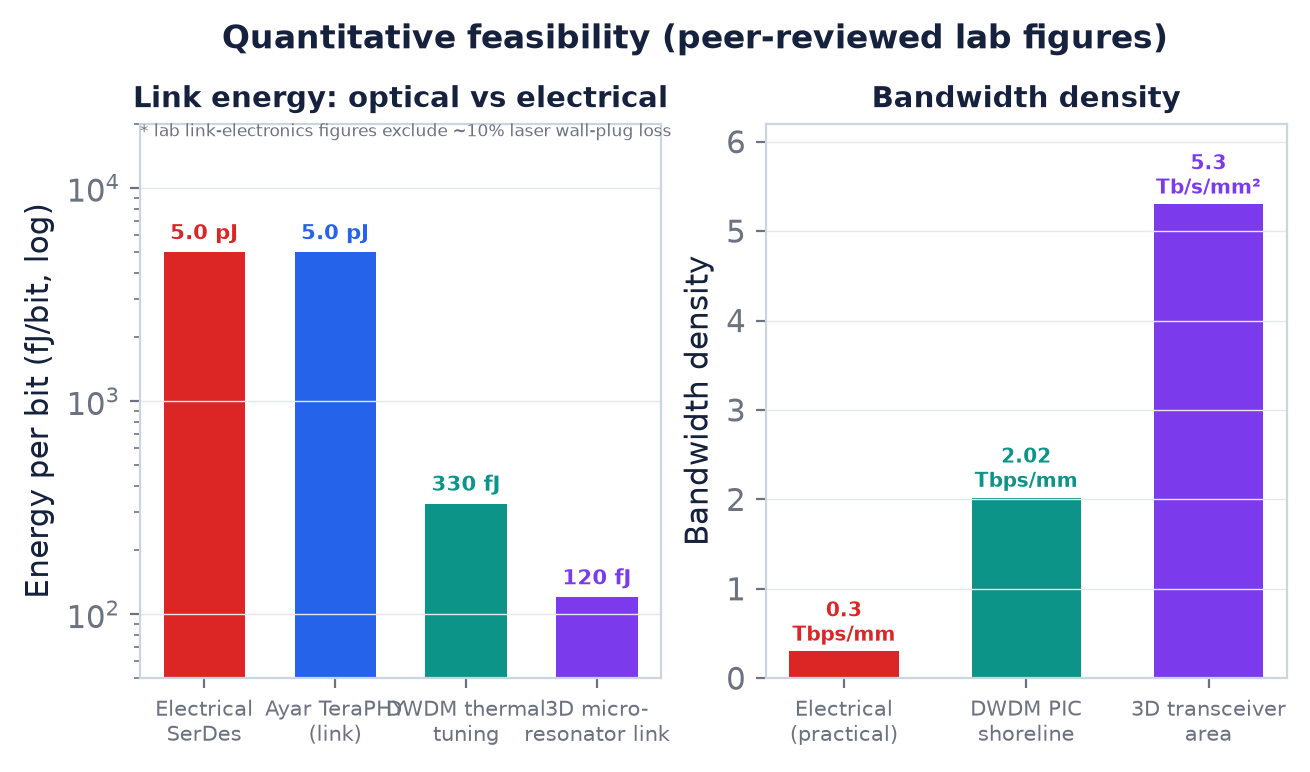
Honest asterisk. These lab figures exclude the laser at ~10% wall-plug efficiency, plus the DAC/ADC/SerDes stack. System-level pJ/bit is materially higher. The advantage is real but smaller than the link-electronics numbers alone imply.
Refuted — do not cite. The combined claim of ">2 Tbps/mm AND sub-1 pJ/bit as a proven at-scale die-to-die path" was killed 0–3. Each number holds individually; the composite at-scale claim does not.
4.3 The disaggregation-latency math — the load-bearing trade-off
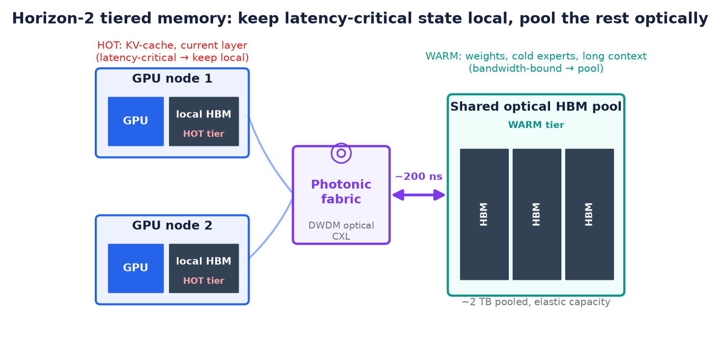
Local HBM access is ~tens of ns; the Celestial Gen1 pooled figure is ~200 ns. That ~150 ns adder is invisible to bandwidth-bound streaming (weight/activation traffic) but a real tax on latency-bound random access (KV-cache, attention during decode). This single number decides which workloads tolerate pooled VRAM — and it rests on one vendor figure, so validate it before committing.
5. The Architected Resolution — Three Horizons
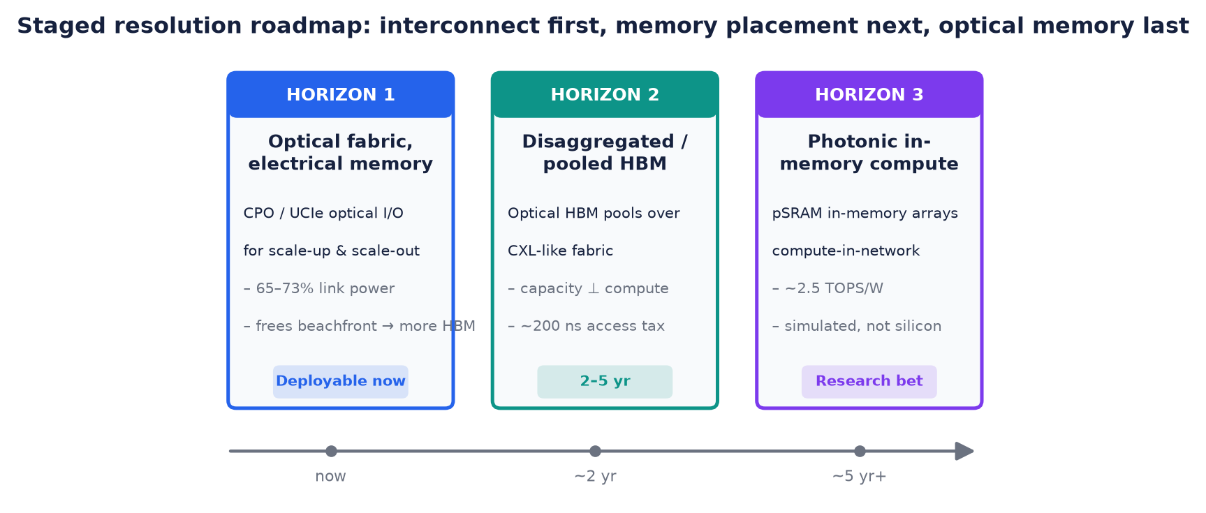
Horizon 1 (now → ~2 yr): optical fabric, electrical memory
Design. Keep HBM local and electrical; replace scale-up/scale-out SerDes with UCIe optical I/O chiplets and CPO switching. Standardize on a UCIe electrical interface + protocol-agnostic optical PHY so the same optics carry CXL / NVLink / UALink / Ethernet.
Payoff. ~65–73% link-power reduction (Meta measured 65%: 5.4 W vs 15 W per 800G), longer reach, and freed beachfront → more in-package HBM. More effective VRAM without touching memory semantics.
Trade-off. Doesn't break the fixed HBM:compute ratio yet, and introduces CPO serviceability risk (§6).
Horizon 2 (~2–5 yr): optically disaggregated / pooled HBM
Design. Break HBM out of the package into optically-attached memory pools over CXL-like fabrics (Photonic Fabric / Marvell CXL-switch template). Compute nodes draw capacity elastically from a shared pool.
Payoff. The actual "photonic VRAM" fix — capacity scales independently of the GPU die; right-size memory per job and stop stranding HBM.
Trade-off & mitigation. The ~200 ns tax. Architect a tiered memory model — hot/latency-critical state (KV-cache, current layer) stays local; warm/bandwidth-bound state (weights, cold experts, long context) lives in the optical pool.
Horizon 3 (5 yr+, research bet): photonic in-memory / compute-in-network
Design. Push compute into the optical/memory domain — pSRAM in-memory arrays (~0.9–1.5 TOPS, ~2.5 TOPS/W, 0.5 pJ/switch, fabricated in GF 45SPCLO) and compute-in-network reductions on the fabric.
Status. Bitcell fabricated, but system throughput is simulated, not silicon-measured. A hedge / watch item, not a plan.
6. Risks — What Actually Kills This
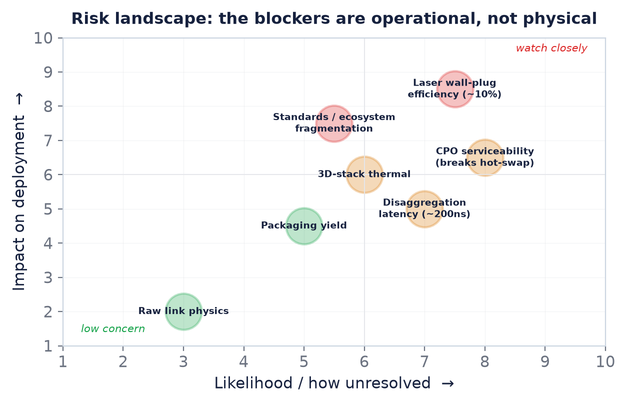
Every risk below was independently verified. The decisive blockers are operational, not physical.
- Laser wall-plug efficiency ~10% (III-V-on-Si DFB ~16%). The unglamorous dominant loss; every "sub-pJ/bit link" quietly excludes it. Mitigation: external / shared laser banks (ELSFP).
- CPO breaks the hot-swap model. A failed embedded optical engine can force replacing a whole package/board vs a front-panel pluggable — an operational-economics problem. Mitigation: detachable optical sub-assemblies / external-laser FRUs.
- 3D-stack thermal. Vertical stacking concentrates heat and can cap optical density before device physics does; 2.5D/lateral integration degrades more gracefully. (The stronger claim that thermal is the single ceiling was refuted 0–3.)
- Ecosystem fragmentation. Open question whether the market converges on UCIe-optical + CXL/UALink (multi-vendor pools) or fragments into proprietary fabrics (NVLink, Marvell/Celestial). A bet-the-architecture standards risk.
7. Claims Deliberately NOT Relied Upon (Adversarially Refuted)
These attractive-sounding claims did not survive verification and are excluded from the recommendations:
| Refuted claim | Vote | Note |
|---|---|---|
| Celestial Photonic Fabric ">2× the power efficiency of copper" | 1–2 | Vendor claim, unproven |
| ">2 Tbps/mm AND sub-1 pJ/bit at scale" as one proven package | 0–3 | Components hold, composite doesn't |
| Heterogeneous-CPO yield = product of die yields, capping scale | 1–2 | Overstated |
| "Thermal, not photonics, sets the ceiling" | 0–3 | Serious constraint, not a hard wall |
Also treat vendor performance numbers (Celestial 16 Tbps / 25×, Ayar 8 Tbps) as architecturally verified but not independently benchmarked.
8. Concrete Recommendations
- Adopt on the fabric first, memory later. Optical I/O + CPO for scale-up/scale-out is the only rung with real ROI now (65–73% link power, freed beachfront → more local HBM). Do this independent of any disaggregation bet.
- Standardize on UCIe-optical + CXL semantics. The only path to multi-vendor optically-pooled memory; hedges fragmentation risk. Avoid welding to one proprietary fabric.
- Characterize the ~200 ns tax on your workloads before pooling. Bandwidth-bound → pool aggressively. Latency-bound decode → keep local. Build the tiered hot/warm model explicitly.
- Budget for laser efficiency and serviceability, not just link pJ/bit. These, not device physics, are what stall deployment. Require external-laser / FRU-serviceable designs.
- Fund photonic in-memory compute as a watch-item only. No silicon-validated system yet.
9. Open Questions to Resolve Next
- True end-to-end, system-level energy-per-bit of optical links including laser wall-plug power (~10%) versus HBM4/HBM3E electrical access — does the sub-pJ/bit advantage survive full accounting?
- How badly does the ~200 ns pooling latency degrade real random-access workloads (KV-cache, attention), and which workloads tolerate pooled HBM vs require local HBM?
- Can CPO serviceability and laser reliability reach datacenter-acceptable FRU economics, and what MTBF/repair thresholds must be met before hyperscalers replace pluggables at scale?
- Will the ecosystem converge on one standards stack (UCIe-optical + CXL/UALink) or fragment into proprietary fabrics?
Key Sources
- Gholami et al., AI and Memory Wall, IEEE Micro 2024 — arXiv:2403.14123
- Celestial AI, Photonic Fabric for Memory & Compute Disaggregation, OFC 2025 W3D.1 — Optica
- Marvell–Celestial AI acquisition release (Dec 2025) — investor.marvell.com
- Ayar Labs — world's first UCIe optical chiplet (Mar 2025) — BusinessWire
- Columbia Lightwave, IEEE CICC 2024 (shoreline density, thermal-tuning energy) — PDF
- Nature Photonics 2025 (120 fJ/bit, 5.3 Tb/s/mm²) — nature.com
- Nature Communications silicon-photonics roadmap (laser WPE) — PMC10811194
- IET Optoelectronics 2021 (pluggable-vs-CPO fork) — Wiley
- pSRAM in-memory compute — arXiv:2602.00892